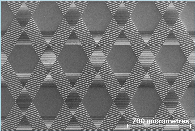
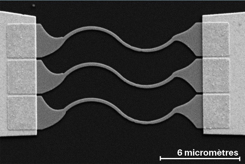
A nanometre is one billionth of a metre, a hair cut 100,000 times, in short, it’s so small that you can’t see it or feel it. Yet nano is made all day long all over the world. Nano is all around us. As I write these words, I am using my computer, whose processor and screen are full of nano or micrometer sized objects.
How can we make such small things in a controlled way?
There are many ways to do this, but today I’m going to talk about a process called lithography.
This is a technique that kindergarten pupils know well: stencilling. With illustrations it will be easier, so here is what a lithography process is.
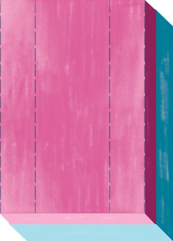
It all starts with the support on which the nano-object is to be fabricated. This support is often called “the substrate” in our jargon. It is chosen for its physical and chemical properties (transparent, conductive, hydrophobic, etc.).
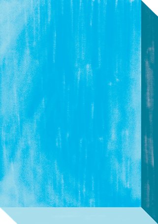
For us, here it will be this blue rectangular plate (it can represent glass, silicon, etc)
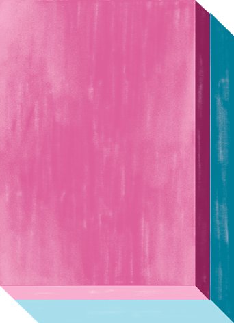
A lithography process starts by depositing a resist (here in pink) on the substrate.
A resist is a slightly viscous liquid which has particular properties: UV light modifies its molecular structure!
To deposit it, a few drops are poured onto the substrate and the whole thing is spun at several thousand rotation per minute. This step is called “spin-coating“.
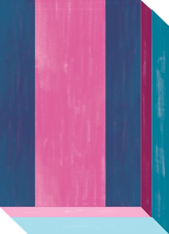
Now comes the stencil stage! Except that in our jargon we don’t call it a stencil but a mask (yes, that’s not really jargon ;-)).
The idea is that some parts are opaque and others transparent to light.
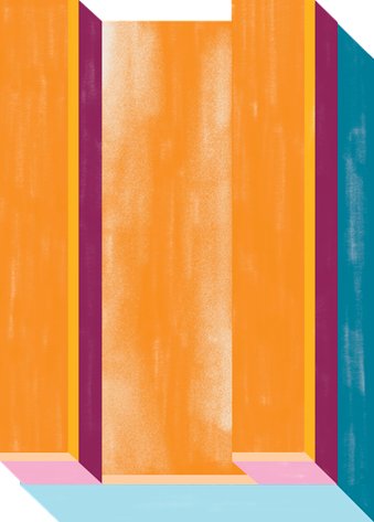
The shape of the openings of this mask is the pattern that we want to reproduce. Here we have chosen a line, but it can be any shape!
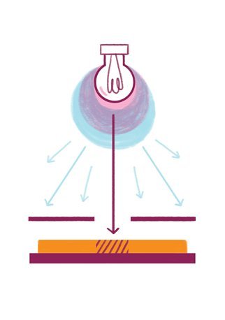
Once the mask has been placed, the whole [mask – resin – substrate] is illuminated with UV light.
This light has been chosen to change the molecular structure of the illuminated resist.
A more rigorous way of saying this is that the wavelength of the light allows the polymer that makes up the resist to cross-link.
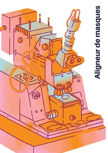
A mask aligner is used to illuminate the resin – we call it “insolation“. This instrument allows the mask to be positioned correctly in relation to the substrate, but also to be pressed against the resist to avoid shadow effects. Above all, it allows the duration of the exposure to be controlled.
Since the beginning, I have been trying to explain how to make nano-objects. But what I have described so far – optical lithography – is more about making micro-objects.
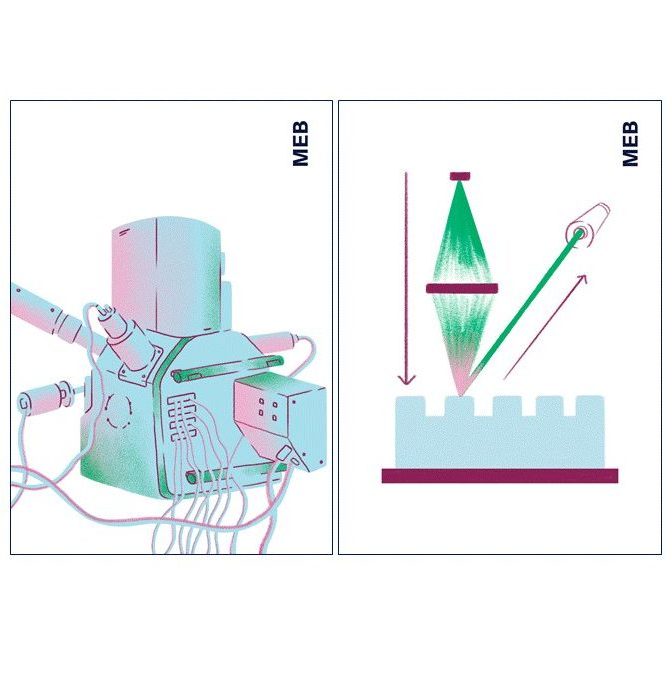
If you want to go to the nano scale (1,000 times smaller), you will use a very similar technique but where the light and the mask are replaced by an electron beam.
The mask aligner is then replaced by a scanning electron microscope (SEM) whose electron beam is used like a brush to draw the desired pattern on an electro-sensitive resin
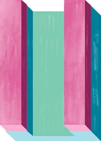
Let’s get back to the point! Once it is exposed, the molecular structure of the exposed resist is no longer the same as that of the masked resist. This is important because the exposed resist can be dissolved in a liquid called a developer.
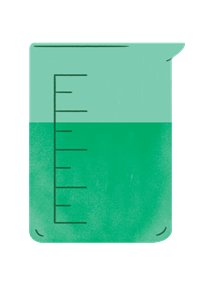
In fact, the sample is dipped in a beaker and when it comes out the exposed part will have been dissolved.
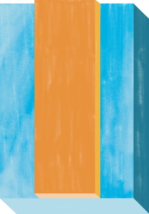
And here it is! A very small opening (micro for optical lithography and nano for electronic lithography) has been made in the resist…
The lithography itself stops here, but making holes in the resist is not very interesting, so here are the two steps that can follow.
1
If the objective is to make trenches in the substrate. It is then necessary to dig, i.e. to remove material.
For this purpose, an etching frame is used, for example. This is an enclosure in which it is possible to control the pressure and the gases present. The idea is to precipitate this gas against the sample to remove material either by an abrasion effect or by chemical reaction with the surface
At the end of this step, the substrate has been etched but there is also some resist left. To dissolve it, it is simply soaked in a beaker filled with acetone.
2 Another possibility is to make a relief structure on the substrate. We therefore seek to add material.
Here again, there are different techniques available. One of the most common is evaporation.
The sample is inserted in an instrument very similar to the etching instrument in that the pressure and gases present are very finely controlled. The difference is that there is also a metal heated sufficiently for it to evaporate.
The sample is placed in this atomic vapour and is soon completely covered.
The evaporated material covers both the substrate and the resist residue.
Here again, the sample is soaked in a beaker of acetone to dissolve the resist.
This operation is called “lift-off“.
Now you know how to make objects without seeing and handling them!
I hope that these superb illustrations by Clara Hinoveanu have helped you to understand. The images are taken from a project I did with the “physics reimagined” team: the nano factory, which you can find here
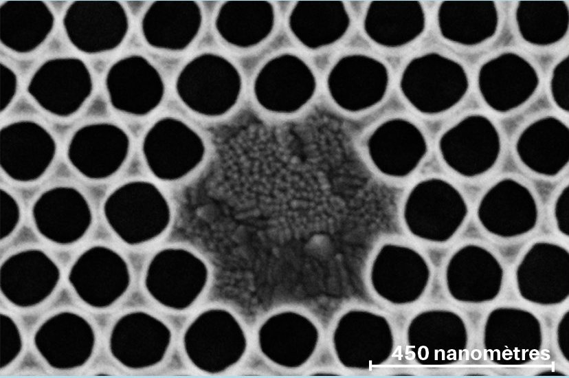
To finish, and to show you how powerful these techniques are, here is a small gallery of objects made by lithography
Post Scriptum
For those of you who arrived here by seeing a short video of me dressing in a blue suit, you may be wondering what this has to do with anything.
Lithography means making objects that are so small that they are smaller than the cells in our skin, the diameter of our hair and even the threads in the fabric of our clothes. If one of these dusts were to fall on our sample, that would be the end of nanos!
This is why nano- and micro-fabrication is done in a so-called clean environment where the number and size of dust is controlled. It is required to dress in a suit to avoid spreading dust in the clean room facility.

